
Revolutionizing semiconductor fab operations with AI
The demand for semiconductors is rising, with the total semiconductor device market expected to reach $1.6 trillion by 2030. As production ramps up, stakeholders across the semiconductor supply chain can use AI to optimize costs and improve efficiency. Foundries and integrated device manufacturers (IDMs) can use AI to optimize the amount of capital they spend on building new fabrication centers (fabs), reduce procurement costs, and improve productivity. If fully scaled across operations and processes, AI could save nearly $134 billion in functional costs in the semiconductor industry in just five to seven years.
To fully benefit from the opportunities presented by AI, semiconductor companies must take a structured approach to assess their digital maturity, identify and prioritize high-impact use cases, and scale transformation efforts systematically. This article discusses the potential of and application for AI in fab building, fab procurement spend optimization, and fab operations efficiency enhancements.
Applications for AI in semiconductor fabrication
In addition to advancing the sector technologically, integrating AI into the semiconductor industry would strategically optimize capital deployment when new fabs are built and minimize operating costs by improving productivity and addressing challenges in spend management, sourcing, and risk mitigation. These tools could have the biggest impact on semiconductor manufacturing processes, leading to as much as $45 billion in savings in as few as four years (exhibit).
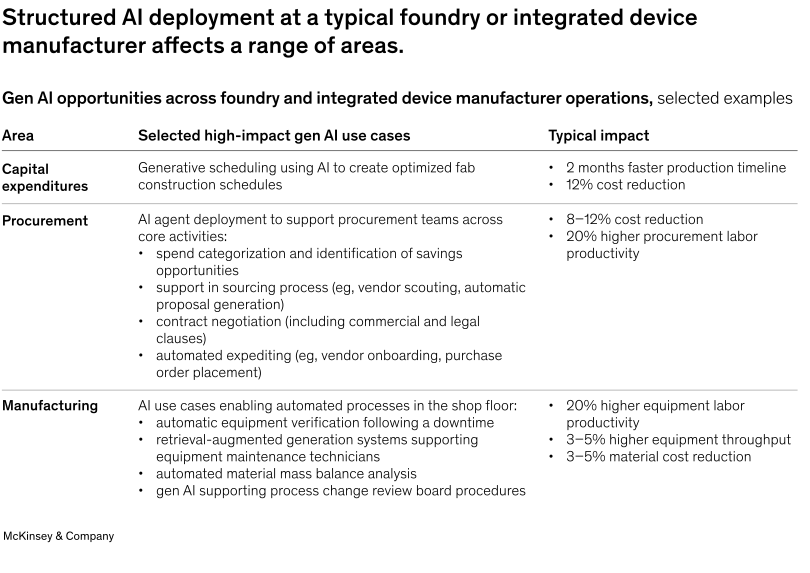
Our research has found that AI can be especially effective when applied to six stages in the semiconductor construction, procurement, and manufacturing processes.
Generative scheduling during fab construction
Generative scheduling uses AI to create optimized construction schedules. It considers hundreds of potential physical, spatial, and temporal constraints to allow project teams to identify the most efficient and cost-effective strategies. This system tests on-site scenarios and responds to changes in real time, proactively updating workstreams in response so teams can ensure projects remain on track and within budget. In terms of project management, generative scheduling can explore approaches such as right-to-left or middle-out to determine the most efficient strategy. Teams can align their activities with project milestones and site constraints to minimize delays and disruptions.
The model considers factors such as labor availability, equipment specifications, and material procurement to optimize resource allocation on sites. For example, it can evaluate how teams are using cranes with different capacities or whether modular construction techniques could improve efficiency. By simulating multiple scenarios, generative scheduling helps identify potential risks and develops mitigation strategies, which reduces uncertainties and ensures smoother project execution, even in the face of supply chain disruptions or labor shortages.
Generative scheduling has demonstrated significant potential in reducing build timelines and costs. For example, a major semiconductor fab project in North America used this approach to identify more than 90 optimization opportunities, including ways the team could improve resource utilization. Generative scheduling allowed the team to reduce their timeline by two months (a 10 percent decrease) and reduced costs by 12 percent (see sidebar, “How generative scheduling can optimize a company’s project execution”).
Agents during procurement
AI agents can be used during procurement to optimize categorization, sourcing, contract negotiations, and purchasing.
Categorization. Agents can provide real-time, granular insights into procurement data to optimize spending strategies. Category agents, which help source and analyze category-specific data to make quick decisions, can help managers improve efficiencies and capture untapped value across procurement functions. These agents can help companies categorize spending with more than 95 percent accuracy, identify cost-saving opportunities, and optimize supplier contracts. This precision allows semiconductor firms to reduce costs by up to 10 percent while improving operational efficiency by about 20 percent.
Sourcing. Sourcing in the semiconductor industry is complex, involving specialty suppliers that can provide complex or rare gases, chemicals, and equipment. Sourcing agents are streamlining this process by using AI to scout and discover suppliers, automatically generating request proposals, and optimizing award allocation for suppliers of critical chemicals and specialty gases. Owners and operators can save up to 50 percent of the time they’d typically spend on these activities by using sourcing agents, making sourcing one of the biggest areas of opportunity for AI applications to pay off.
Contract negotiations. In the semiconductor industry, contracts often involve intricate terms related to intellectual property, exclusivity, and supply guarantees. Contract negotiation agents can help automate the drafting, review, and comparison of contracts, which not only reduces errors and ensures compliance but also can save up to 30 percent of the time these associated procurement activities typically take.
Specifically, contract negotiation agents can help teams more easily build should-cost models based on engineering drawings, bills of materials, cost sheets, and specs for physical teardowns. Manually, this process is time-intensive, so it is rarely applied in the semiconductor industry. With AI-enabled solutions, semiconductor companies can run hundreds of models at once within a category to determine which individual products or suppliers drive the highest costs. Moreover, aggregated category-wide insights show savings for high-value representative components as well as high-volume, low-value purchases from suppliers, enabling cost savings between 5 and 9 percent.
Purchasing. Purchase agents can help place orders, track inventory levels, and manage supplier relationships. These tools can automate purchase order handling, supplier qualification and onboarding, exception management, and vendor statement reconciliation, allowing semiconductor owners and operators to save 5 to 15 percent and improve purchasing efficiency by about 30 percent. Moreover, agents may also further optimize sales and operations planning (S&OP) to become more cost-efficient over time.
Automated verifications during equipment downtimes
Equipment downtime is a major source of inefficiency in semiconductor manufacturing. Equipment failures require thorough assessments from maintenance workers to diagnose causes, check for damage, and identify the potential impacts on the quality of outputs. Manually completing these processes can significantly extend downtimes, which disrupts production schedules and increases costs.
AI-based verification systems minimize the need to manually run the assessments that follow downtime and help to resume production faster. AI can automatically run diagnoses and determine whether equipment can be reintegrated into production based on a standard set of decision rules, enabling faster and more consistent judgments. On average, machine downtime can be reduced by 30 percent, which equates to about 15 hours saved per failure event.
Moreover, with AI monitoring, the quality and consistency of wafers can be monitored throughout the manufacturing process, eliminating the need to create wafers specifically to test quality assurance. As such, materials can be used on production wafers only, which saves time and reduces material waste, further enhancing efficiency.
Large language models during maintenance
Across different applications, large language models (LLMs) can help improve the efficiency of shop floor operations. They can provide maintenance information quickly and disseminate best practices across different fabs, which helps maintenance technicians become more efficient and minimizes their chance of errors. Applying LLMs to existing capabilities can increase labor productivity by up to 35 percent.
Printed equipment-maintenance manuals are often long and complex; locating relevant information in these documents can be time-consuming and fallible, especially when technicians are under pressure to resolve issues quickly. Technicians can interact with LLMs through simple, natural language queries, which eliminates the need to search for information. LLMs can instantly retrieve relevant sections of equipment manuals and process documentation as well as data about previous issues and how they were resolved across the full fab network. Complex (and less frequent) issues can be resolved faster, and junior operators with less expertise can have a consistent resource and knowledge base, which helps to streamline troubleshooting and reduce the likelihood of errors.
Beyond information retrieval, LLMs can offer advanced chatbot functionalities powered by natural language processing and reasoning capabilities. These features provide solutions based on context, ensuring that technicians receive actionable insights tailored to the specific issue they are addressing. Additionally, LLMs support prescriptive maintenance, which builds on predictive maintenance by identifying the most effective actions to resolve problems efficiently.
The impact of these innovations is substantial. LLMs can free up to 20 percent of maintenance technicians’ time, allowing them to focus on higher-value tasks that drive greater operational impact. By minimizing errors during maintenance, LLMs also help avoid further downtime or wafer scrap, ensuring smoother operations and reducing costs. In total, the integration of LLMs within the maintenance process can reduce total cash costs per mask layer by up to 3 percent. Furthermore, these tools address labor shortages by accelerating the upskilling and reskilling of technicians, equipping them with the knowledge and confidence to navigate increasingly complex manufacturing environments.
Automated mass balance analysis during manufacturing
Material consumption deviations during manufacturing processes can lead to significant inefficiencies, particularly in high-cost inputs such as chemicals, chemical mechanical planarization slurry, and photochemicals. Automated mass balance analysis can help fabs identify and eliminate waste in material consumption.
By linking live data on procured amounts, actual usage, and recipe requirements, automated systems can detect anomalies and pinpoint inefficiencies in the semiconductor manufacturing process. This approach enables fabs to optimize material usage, generating savings on material costs of 5 to 10 percent. These savings not only reduce costs but also contribute to more-sustainable manufacturing practices.
Gen AI during process change review board procedures
Another impactful application of AI in semiconductor manufacturing quality control is in process change review board (PCRB) processes. PCRBs oversee the qualification of manufacturing processes, including the review of steps and recipes, as well as performance monitoring of multiple wafer lot qualifications. Traditionally, these activities are time-intensive (lasting nine to 12 months) and involve extensive experiment design, data analysis, and performance assessments.
Gen AI can streamline this process by providing the team in charge of process review with additional insights from previous similar process changes, such as the ideal number of wafer lots to be tested and the high-priority parameters to be considered. The impact of these advancements can be significant. PCRB approval times can be reduced by up to 20 percent, while engineering team hours on lower-value-added activities (such as testing planning) can be cut by a similar margin. This enables fabs to bring new processes online faster and with greater confidence, enhancing overall operational agility.
Where semiconductor companies can start with AI
There are several valuable opportunities today to deploy AI in semiconductor fab building, procurement, and operations processes. Deploying these technologies requires foundries and IDMs to apply a clear ambition for AI and a structured road map for implementation. Companies must first articulate the outcomes they seek—for example, improved build timelines, optimized capital deployment, cost reductions during procurement, higher throughputs, improved wafer quality, or reduced downtimes—and then design an approach that links technical capabilities to business priorities and set guardrails for the associated opportunities.
A proven methodology consists of four key activities in two main phases:
- Phase 1: AI strategy and use case selection. In this phase, companies should develop a definition of their overall AI strategy and select the most appropriate use cases.
- Phase 2: Implementing pilots and establishing change management governance. In this phase, companies should execute and scale their prioritized pilot projects. They should also establish governance and a structured change management road map.
These two phases ensure companies can capture early wins while mitigating risk and scaling capabilities across fabs.
Phase 1: AI strategy and use case selection
The first stage defines how AI aligns with business and innovation priorities. Organizations should decide which processes to target, the expected benefits (such as scrap reduction or cycle time improvements), and the scale of the AI deployment. At this stage, technical considerations, such as data modalities, model architectures, and cybersecurity requirements, should be addressed. Business units’ readiness to integrate AI into operations should also be assessed (for example, their familiarity with AI tools and the ease at which LLMs can be integrated within a company’s IT architecture), and fallback procedures should be set in place in case of underperformance.
Once the AI strategy is formed, companies should select the most appropriate use cases to demonstrate value early and build internal momentum. The goal is to balance quick wins with scalable opportunities, ensuring each initiative aligns with broader operational goals. Organizations should typically assess use cases based on their impact or feasibility, taking into account additional considerations such as data availability and scalability across processes and fabs. Furthermore, organizations can cluster the use cases by their area of impact, including predictive maintenance, work-in-progress management, or equipment downtime reduction, to ensure comparability.
Companies typically scan 40 to 50 use cases, narrowing the list to about ten high-priority ones that can ensure quick wins and show potential to scale. Among these, one or two high-impact pilots can be prioritized as proof of concept. Across these activities, cross-functional collaboration that blends data science expertise with process knowledge is critical to validate the feasibility of each project and anticipate roadblocks early.
Phase 2: Implementing pilots and establishing change management governance
Selected pilots begin with data validation and model prototyping and can be tested on targeted fab build projects, procurement spend categories, and fab process steps. Iterative feedback from engineers and operators can help leaders to fine-tune models and interfaces. KPI dashboards can be established to measure performance against key metrics, such as timeline acceleration, reductions in spending, throughput gains, yield improvement, or downtime reduction. Once validated from a technical, operational, and financial perspective, solutions can be integrated into IT and data architecture and progressively scaled across a fab build project, spend categories, and workflows, tools, and sites.
Sustained adoption, however, requires governance and change management. C-level leaders can establish groups—often led by operations or process engineering heads—to steer these efforts and to oversee the rollout of AI initiatives and track results. Governance should then be reinforced at regular cadences, such as during performance reviews (based on KPIs around AI adoption, for example) and progress updates. Change management is vital to clearly communicate goals to operators, provide hands-on training and demos, build tailored incentive structures, and provide employees visible sponsorship from senior leadership. These measures build trust and embed AI as a core tool to be used across fabs.
Beyond the $60 billion savings potential AI has on improving operations, capital deployment, and procurement, a further $74 billion could be gained by using AI to enhance productivity and efficiency across research and development, material discovery, chip design, and sales and pricing. By combining disciplined strategy-setting, careful use-case selection, robust pilots, and strong governance, semiconductor companies can move beyond experiments and realize sustainable benefits from AI.